2020. 3. 11. 10:03ㆍAnalog/Filters
출처 : https://www.electronics-tutorials.ws/filter/band-stop-filter.html
Band Stop Filter
A band Stop Filter known also as a Notch Filter, blocks and rejects frequencies that lie between its two cut-off frequency points passes all those frequencies either side of this range


By combining a basic RC low-pass filter with a RC high-pass filter we can form a simple band-pass filter that will pass a range or band of frequencies either side of two cut-off frequency points. But we can also combine these low and high pass filter sections to produce another kind of RC filter network called a band stop filter that can block or at least severely attenuate a band of frequencies within these two cut-off frequency points.
The Band Stop Filter, (BSF) is another type of frequency selective circuit that functions in exactly the opposite way to the Band Pass Filter we looked at before. The band stop filter, also known as a band reject filter, passes all frequencies with the exception of those within a specified stop band which are greatly attenuated.
If this stop band is very narrow and highly attenuated over a few hertz, then the band stop filter is more commonly referred to as a notch filter, as its frequency response shows that of a deep notch with high selectivity (a steep-side curve) rather than a flattened wider band.
Also, just like the band pass filter, the band stop (band reject or notch) filter is a second-order (two-pole) filter having two cut-off frequencies, commonly known as the -3dB or half-power points producing a wide stop band bandwidth between these two -3dB points.
Then the function of a band stop filter is too pass all those frequencies from zero (DC) up to its first (lower) cut-off frequency point ƒL, and pass all those frequencies above its second (upper) cut-off frequency ƒH, but block or reject all those frequencies in-between. Then the filters bandwidth, BW is defined as: (ƒH – ƒL).
So for a wide-band band stop filter, the filters actual stop band lies between its lower and upper -3dB points as it attenuates, or rejects any frequency between these two cut-off frequencies. The frequency response curve of an ideal band stop filter is therefore given as:
Band Stop Filter Response
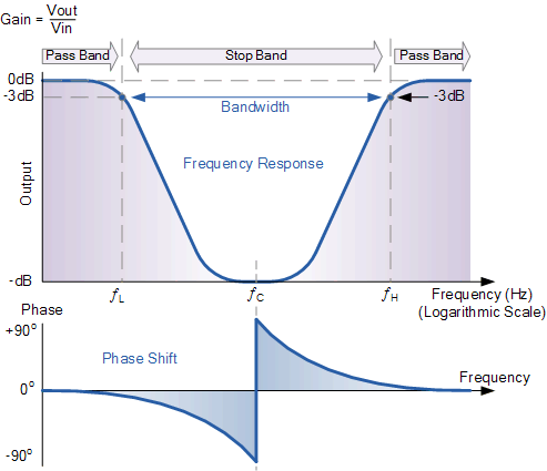
We can see from the amplitude and phase curves above for the band pass circuit, that the quantities ƒL, ƒH and ƒC are the same as those used to describe the behaviour of the band-pass filter. This is because the band stop filter is simply an inverted or complimented form of the standard band-pass filter. In fact the definitions used for bandwidth, pass band, stop band and center frequency are the same as before, and we can use the same formulas to calculate bandwidth, BW, center frequency, ƒC, and quality factor, Q.
The ideal band stop filter would have infinite attenuation in its stop band and zero attenuation in either pass band. The transition between the two pass bands and the stop band would be vertical (brick wall). There are several ways we can design a “Band Stop Filter”, and they all accomplish the same purpose.
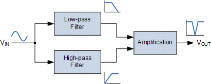
Generally band-pass filters are constructed by combining a low pass filter (LPF) in series with a high pass filter (HPF). Band stop filters are created by combining together the low pass and high pass filter sections in a “parallel” type configuration as shown.
Typical Band Stop Filter Configuration
The summing of the high pass and low pass filters means that their frequency responses do not overlap, unlike the band-pass filter. This is due to the fact that their start and ending frequencies are at different frequency points. For example, suppose we have a first-order low-pass filter with a cut-off frequency, ƒL of 200Hz connected in parallel with a first-order high-pass filter with a cut-off frequency, ƒH of 800Hz. As the two filters are effectively connected in parallel, the input signal is applied to both filters simultaneously as shown above.
All of the input frequencies below 200Hz would be passed unattenuated to the output by the low-pass filter. Likewise, all input frequencies above 800Hz would be passed unattenuated to the output by the high-pass filter. However, and input signal frequencies in-between these two frequency cut-off points of 200Hz and 800Hz, that is ƒL to ƒH would be rejected by either filter forming a notch in the filters output response.
In other words a signal with a frequency of 200Hz or less and 800Hz and above would pass unaffected but a signal frequency of say 500Hz would be rejected as it is too high to be passed by the low-pass filter and too low to be passed by the high-pass filter. We can show the effect of this frequency characteristic below.
Band Stop Filter Characteristics

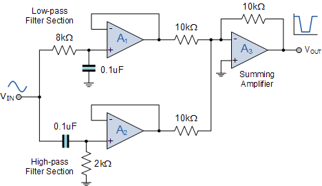
The transformation of this filter characteristic can be easily implemented using a single low pass and high pass filter circuits isolated from each other by non-inverting voltage follower, (Av = 1). The output from these two filter circuits is then summed using a third operational amplifier connected as a voltage summer (adder) as shown.
Band Stop Filter Circuit
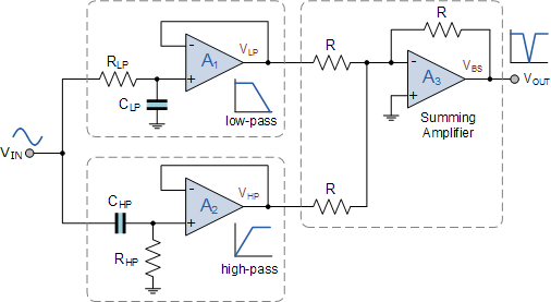
The use of operational amplifiers within the band stop filter design also allows us to introduce voltage gain into the basic filter circuit. The two non-inverting voltage followers can easily be converted into a basic non-inverting amplifier with a gain of Av = 1 + Rƒ/Rin by the addition of input and feedback resistors, as seen in our non-inverting op-amp tutorial.
Also if we require a band stop filter to have its -3dB cut-off points at say, 1kHz and 10kHz and a stop band gain of -10dB in between, we can easily design a low-pass filter and a high-pass filter with these requirements and simply cascade them together to form our wide-band band-pass filter design.
Now we understand the principle behind a Band Stop Filter, let us design one using the previous cut-off frequency values.
Band Stop Filter Example No1
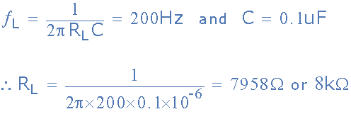
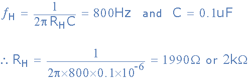
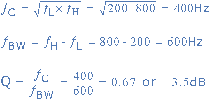
Design a basic wide-band, RC band stop filter with a lower cut-off frequency of 200Hz and a higher cut-off frequency of 800Hz. Find the geometric center frequency, -3dB bandwidth and Q of the circuit.
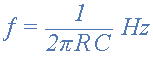
The upper and lower cut-off frequency points for a band stop filter can be found using the same formula as that for both the low and high pass filters as shown.
Assuming a capacitor, C value for both filter sections of 0.1uF, the values of the two frequency determining resistors, RL and RH are calculated as follows.
Low Pass Filter Section
High Pass Filter Section
From this we can calculate the geometric center frequency, ƒC as:
Now that we know the component values for the two filter stages, we can combine them into a single voltage adder circuit to complete our filter design. The magnitude and polarity of the adders output will be at any given time, the algebraic sum of its two inputs.
If we make the op-amps feedback resistor and its two input resistors the same values, say 10kΩ, then the inverting summing circuit will provide a mathematically correct sum of the two input signals with zero voltage gain.
Then the final circuit for our band stop (band-reject) filter example will be:
Band Stop Filter Design
We have seen above that simple band stop filters can be made using first or second order low and high pass filters along with a non-inverting summing op-amp circuit to reject a wide band of frequencies. But we can also design and construct band stop filters to produce a much narrower frequency response to eliminate specific frequencies by increasing the selectivity of the filter. This type of filter design is called a “Notch Filter”.
Notch Filters
Notch filters are a highly selective, high-Q, form of the band stop filter which can be used to reject a single or very small band of frequencies rather than a whole bandwidth of different frequencies. For example, it may be necessary to reject or attenuate a specific frequency generating electrical noise (such as mains hum) which has been induced into a circuit from inductive loads such as motors or ballast lighting, or the removal of harmonics, etc.
But as well as filtering, variable notch filters are also used by musicians in sound equipment such as graphic equalizers, synthesizers and electronic crossovers to deal with narrow peaks in the acoustic response of the music. Then we can see that notch filters are widely used in much the same way as low-pass and high-pass filters.
Notch filters by design have a very narrow and very deep stop band around their center frequency with the width of the notch being described by its selectivity Q in exactly the same way as resonance frequency peaks in RLC circuits.
The most common notch filter design is the twin-T notch filter network. In its basic form, the twin-T, also called a parallel-tee, configuration consists of two RC branches in the form of two tee sections, that use three resistors and three capacitors with opposite and opposing R and C elements in the tee part of its design as shown, creating a deeper notch.
Basic Twin-T Notch Filter Design
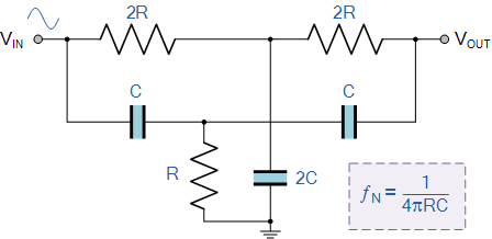
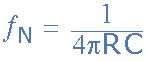
The upper T-pad configuration of resistors 2R and capacitor 2C form the low-pass filter section of the design, while the lower T-pad configuration of capacitors C and resistor R form the high-pass filter section. The frequency at which this basic twin-T notch filter design offers maximum attenuation is called the “notch frequency”, ƒN and is given as:
Twin-T Notch Filter Equation
Being a passive RC network, one of the disadvantages of this basic twin-T notch filter design is that the maximum value of the output (Vout) below the notch frequency is generally less than the maximum value of output above the notch frequency due in part to the two series resistances (2R) in the low-pass filter section having greater losses than the reactances of the two series capacitors (C) in the high-pass section.
As well as uneven gains either side of the notch frequency, another disadvantage of this basic design is that it has a fixed Q value of 0.25, in the order of -12dB. This is because at the notch frequency, the reactances of the two series capacitors equals the resistances of the two series resistors, resulting in the currents flowing in each branch being out-of-phase by 180o.
We can improve on this by making the notch filter more selective with the application of positive feedback connected to the center of the two reference legs. Instead of connecting the junction of R and 2C to ground, (0v) but instead connect it to the central pin of a voltage divider network powered by the output signal, the amount of the signal feedback, set by the voltage divider ratio, determines the value of Q, which in turn, determines to some extent, the depth of the notch.
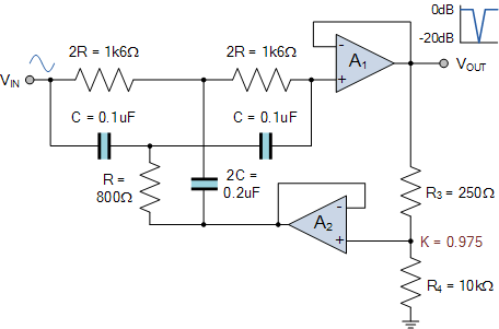
Single Op-amp Twin-T Notch Filter
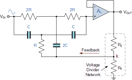
Here the output from the twin-T notch filter section is isolated from the voltage divider by a single non-inverting op-amp buffer. The output from the voltage divider is fed back to “ground” point of R and 2C. The amount of signal feedback, known as the feedback fraction k, is set by the resistor ratio and is given as:
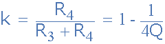
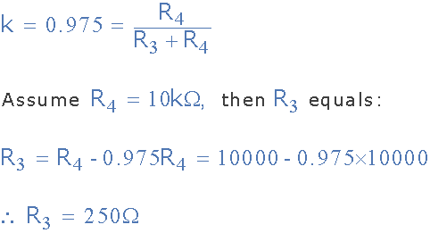
The value of Q is determined by the R3 and R4 resistor ratio, but if we wanted to make Q fully adjustable, we could replace these two feedback resistors with a single potentiometer and feed it into another op-amp buffer for increased negative gain. Also, to obtain the maximum notch depth at the given frequency, resistors R3 and R4 could be eliminated and the junction of R and 2C connected directly to the output.
Band Stop Filter Example No2
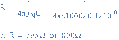
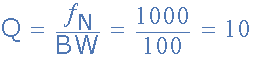
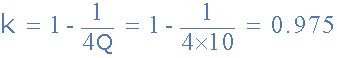
Design a two op-amp narrow-band, RC notch filter with a center notch frequency, ƒN of 1kHz and a -3dB bandwidth of 100 Hz. Use 0.1uF capacitors in your design and calculate the expected notch depth in decibels.
Data given: ƒN = 1000Hz, BW = 100Hz and C = 0.1uF.
1. Calculate value of R for the given capacitance of 0.1uF
2. Calculate value of Q
3. Calculate value of feedback fraction k
4. Calculate the values of resistors R3 and R4
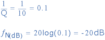
5. Calculate expected notch depth in decibels, dB
Notch Filter Design
Band Stop Filter Summary
We have seen here that an ideal band stop filter has a frequency response which is the inverse of the band-pass filter. Band stop filters block or “reject” frequencies that lie between its two cut-off frequency points ( ƒL and ƒH ) but passes all those frequencies either side of this range. The range of frequencies above ƒL and below ƒH is called the stop band.
Band stop filters accomplish this by summing the outputs of a high pass with that of a low pass filter (especially for the wide band design) with the filters output being the difference. A band stop filter design with a wide stop band is also referred to as a band reject filter and a band stop filter design with a narrow stop band is referred to as a notch filter. Either way, band stop filters are second-order filters.
Notch filters are designed to provide high attenuation at and near a single frequency with little or no attenuation at all other frequencies. Notch filters use a twin-T parallel resistance-capacitance (RC) network to obtain a deep notch. Higher values of Q can be obtained by feeding back some of the output to the junction of the two tees.
To make the notch filter more selective and with adjustable values of Q, we can connect the junction of the resistance and the capacitance in the two tees to the central point of a voltage divider network connected to the filters output signal. A properly designed notch filter can produce attenuation of more than -60dB at the notch frequency.
Band Stop Filters have many uses in electronics and communication circuits and as we have seen here, they can be used to remove a band of unwanted frequencies from a system, allowing other frequencies to pass with minimum loss. Notch filters can be highly selective and can be designed to reject or attenuate a specific frequency or harmonic content generating electrical noise, such as mains hum within a circuit.
'Analog > Filters' 카테고리의 다른 글
| Sallen and Key Filter (0) | 2020.03.11 |
|---|---|
| State Variable Filter (0) | 2020.03.11 |
| Second Order Filters (0) | 2020.03.11 |
| Butterworth Filter Design (0) | 2020.03.11 |
| Active Band Pass Filter (0) | 2020.03.11 |